English
 Spanish
 French
 German
 Italian
 Chinese (Simplified)
 Japanese
 Korean
 Arabic
 Portuguese
- Home Page
- Company Profile
-
Our Products
- Analog Lab Training Modules
- Photo Cell Characteristics Apparatus
- LCR Resonance Circuit with Built in Oscillator
- Ionization Potential of Mercury
- Conversion of Galvanometer to Voltmeter
- Plancks Constant Apparatus (AE206)
- Transistor Characteristics Apparatus
- Transistor Characteristics Apparatus (AE212)
- Diac Characteristics Apparatus
- Conversion of Galvanometer to Ammeter
- Peak Average Rms Value of a AC Signal
- Pentode Valve Characteristics Apparatus
- Photo Transistor Characteristics Apparatus
- Charging and Discharging of Condenser
- LR Circuit With A Source Of Alternating E.M.F
- Hall Effect Experiment Apparatus
- Study of Switching action of a Transistor (BJT)
- Flashing Quenching of Neon Apparatus
- IGBT Characteristics Apparatus
- Tunnel Diode Characteristics Apparatus
- Resistances in Series Parallel Apparatus
- Solar Cell Characteristics Apparatus
- Clipping and Clamping Circuit Apparatus
- LCR Resonance Apparatus
- BH Curve Apparatus with Solenoid
- Half Wave Full Wave and Bridge Rectifier Apparatus
- Plancks Constant Experiment
- UJT Characteristics Apparatus and UJT as Relaxation Oscillator (Combined Model)
- Work Function of Diode (Richardson Law (AE 209)
- PN Junction or Semiconductor Diode Characteristic
- FET Characteristics Apparatus
- PN Junction or Zener Diode or LED Characteristics Apparatus
- Energy Band Gap of PN Junction Diode (AE218)
- Conversion of Galvanometer to Voltmeter and Ammeter
- RC Circuit as High Pass and Low Pass Filters
- Zener Diode Characteristics and Voltage Stabilization
- Thermistor Characteristics Apparatus
- Planck Constant Determination Using LED
- Boltzman Constant Kit
- LDR Characteristics Apparatus
- Biasing Techniques of Transistor (BJT)
- Transformer characteristics Apparatus
- Voltage Doubler and Tripler Circuit
- LCR Impedance Circuit Apparatus
- Quinck`s Tube Method
- Diode Valve Characteristics Apparatus
- Work Function of Diode (Richardson Law (AE 209)
- Triode Valve Characteristics Apparatus
- Resistivity Of Semiconductors by four probe method
- KCL and KVL ( Kirchoff's law)
- Three Terminal voltage Regulator Trainer
- Voltage Regulation using Zener Diode & Transistor
- Study of Voltage Regulation using IC LM 317
- Characteristics of Optoelectronic Devices
- Photo Diode Characteristics Apparatus
- LED Characteristics Apparatus
- Triac Characteristics Apparatus
- MOSFET Characteristics Apparatus
- UJT Characteristics Apparatus
- SCR Characteristics Apparatus
- Ripple Factor Apparatus
- BH Curve Apparatus
- Voltage Stabilization Characteristics of Zener Diode
- Zener Diode Characteristics Apparatus
- PN Junction Diode / Semiconductor Diode Apparatus
- Electronic Component and Valves Mounted On Board
- Voltage Regulation by 78 series voltage regulators
- Rc Transmission Line
- Semiconductor Characteristics Trainer
- Laboratory Power Supplies
- Sodium Vapor Lamp Transformer
- Daniel Cell Substitute Electronic
- Electrophoresis Power Supplies
- Lechlanche Cell Substitute Electronic
- Dual Channel Variable DC Regulated Power Supplies
- Millikans Oil Drop Apparatus Power Supply
- Standard Cell (Electronic)
- IC Regulated Battery Eliminators
- DC Regulated Power Supplies
- DC Power Supplies
- Amplifiers Characteristics
- Transistor Amplifier Circuits (CE CB CC)
- Transistor Push Pull Amplifier / Transformer Coupled Amplifier
- Study of Class A B AB and Push Pull Amplifier
- TRANSISTOR AMPLIFIER TRAINER WITH INBUILT SINE WAVE GENERATOR AND AC MILLI VOLTMETER (CE,CB,CC)
- RC Coupled Amplifier with Function Generator and AC Digital meters
- FET Common Source Amplifier
- Two Stage RC Coupled Transistor amplifier
- Common Emitter Transistor Amplifier
- Common Base Transistor Amplifier
- Common Collector Transistor Amplifier
- Complementary Symmetry Amplifier
- Common Base Amplifier with Function Generator and AC Digital meters
- TRANSFORMER COUPLED (PUSH PULL) AMPLIFIER TRAINER WITH SINE WAVE GENERATOR & Digital Meters
- E-M Experiments
- Oscillators Experiments
- Multivibrators Trainers
- Bread Boards Trainers
- Digital Lab Training Modules
- Logic Gates using Universal gates
- Adder and Subtractor using NAND Gates
- Digital to Analog Converter Kit
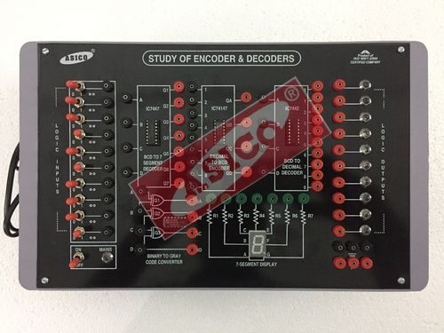
- Study of Encoder and Decoder Circuits
- Analog to Digital Converter kit
- Demorgan Theorem kit
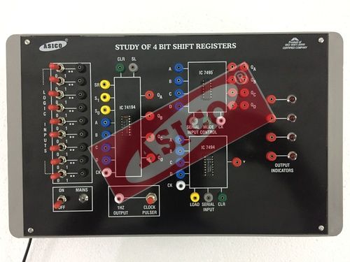
- Study of Left , Right & Programmable Shift Register
- Digital Trainer to verify Half Adder and Full Adder
- Basic Logic Gates using Discrete Component (5 in 1)
- Flip Flops using TTL ICs and NAND Gates
- RAM Circuit using IC 7489
- RS D T JK and JK MASTER SLAVE FLIP FLOP TRAINER
- Verification of Boolean Identity and Demorgans Theorem
- Multiplexer and Demultiplexer 16 bit
- Study of Arithmatic Logic Unit (ALU)
- Study Of 4 Bit Adder And Subtractor
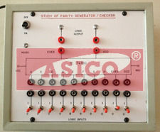
- Study of Parity Generator/Checker
- Study Of Logic Gates Using Ttl ICs 6 in 1
- Study of 4 Bit Counters(Synchronous Asynchronous)
- Study of Logic Gates using TTL ICs (7 in 1)
- TTL IC Characteristics Apparatus
- CMOS IC Characteristics Apparatus
- Filter Circuits
- Communication Lab Training Modules
- Transmission Line Trainer
- Amplitude Modulation and Demodulation using Transistors
- Antenna Trainer
- Pulse Amplitude Modulation and Demodulation Trainer
- Study of Pulse Width Modulation and Demodulation
- Delta Modulation and Demodulaion
- FSK Modulation and Demodulation
- Pulse Position Modulation and Demodulation
- Phase Shift Keying (PSK) Modulation & Demodulation
- Digital Communication Trainer
- Mobile Phone Trainer
- Analog Communication Trainer
- HAMMING CODE (ERROR DETECTION CORRECTION) TRAINER
- FOURIER SYNTHESIS SYSTEM TRAINER
- Data Reformatting & Carrier Demod Receiver Trainer
- Data Formatting and carrier Modulation Transmitter Trainer
- Tdm Pulse Code Demodulation Receiver Trainer
- TDM Pulse Code Modulation Transmitter Trainer
- Delta , Adaptive Delta & Delta Sigma Modulation & Demodulation Trainer
- TDM Pulse Amplitude Modulation Transmitter Trainer
- Dsb Ssb Amplitude Modulation (Am) Transmitter Trainer
- Fibre Optic Communication Trainer
- Frequency Division Multiplexing Modulation
- Pam-pwm-ppm Modulation Demodulation Trainer Kit
- Eprom Trainer
- Analog Signal Sampling and Reconstruction Kit
- Pulse Code Modulation and Demodulation
- Pre-emphasis De-emphasis Trainer
- Phase Modulation & Demodulaion
- Amplitude Shift Keying Modulation & Demodulation
- DSB/SSB AMPLITUDE MODULATION (AM) RECEIVER TRAINER
- Amplitude Modulation and Demodulation
- Frequency Modulation and Demodulation
- Fibre Optic Trainer Analog
- Power Electronic Trainer
- Physics Lab Experimental Setups
- Laser Experimental Set Up (He-Ne Laser)
- SPEED OF SOUND USING KUNDTS TUBE EXPERIMENT
- Resolving Power of a Diffraction Grating Using Spectrometer & Mercury Lamp.
- THERMOSTAT CHARACTERISTICS TRAINER
- Study of Dielectric Constant and Curie Temperature of Ferroelectric Ceramics
- Polarization of Light by Reflection and Determine the Polarizing angle for Air Glass Interface ( Brewster's Law)
- ASICO COUPLING COEFFICIENT OF PIEZOELECTRIC CRYSTAL
- Stefan Constant Apparatus
- e by k using Silicon Transistor
- Stefan Constant Black Body Radiation Apparatus
- Lissajous Figure Apparatus
- Spectrometer Experiment
- Michelson Interferometer
- Choke Characteristics Apparatus
- ASICO Absorption Spectrum of Iodine Vapour
- Temperature Coefficient of Resistance for Platinum Using a Platinum Resistance Thermometer Callender and Griffiths Bridge
- High Resistance Using Substitution Method
- To Determine the Fermi Energy of Copper
- Magnetic Susceptibility By Gouys Balance Experiment
- Laser Experimental Set Up (Diode Laser)
- Determination of Youngs Modulus using Cornus Method.
- Calibration of Voltmeter and Ammeter using Potentiometer
- g by Free Fall Apparatus Experiment
- Ultrasonic Interferometer
- Constant Deviation Spectrometer CDS
- Half Shade Polarimeter Setup
- To Study the Biot Savarts Law
- Measurement Of Magnetoresistance for Semiconductors
- FABRY PEROT INTERFEROMETER
- Newtons Ring Experiment Setup
- Polarisation of Light by Quater Wave Plate Experiment
- PHOTOCONDUCTIVITY EXPERIMENT
- Wavelength of Diode Laser using Diffraction Grating
- Babinet Compensator
- TO DETERMINE THE REFRACTIVE INDEX OF LIQUID BY TOTAL INTERNAL REFLECTION USING WOLLASTON AIR FILM
- Surface Plasmon Resonance (SPR) setup
- Sextant - SXT
- Lamp And Scale Arrangement
- Thermo emf for Copper Iron Thermocouple
- Different types of Gratings and Slits for Laser Experiments
- Laser Grating 3 in 1
- Coulomb Meter
- High Resistance By Leakage Method Experiment
- Velocity of Ultrasonic waves in Kerosene Liquid
- Helium Neon Laser 2mW
- Diode Laser 5mW
- Dielectric Constant for Solids and Liquids
- Dielectric Constant Apparatus (Solids)
- Rydberg Constant Measurement Complete Set-up
- Franck-Hertz Argon Tube Experiment Set
- Calibration of Wattmeter Using Dc Potentiometer
- Malus Law Apparatus
- Spectrum Tube Power Supply
- Fabry-Perot Etalon
- Spot Reflecting Galvanometer
- Ballistic Galvanometer
- Determination of Plancks constant from the LED
- Magnetic Field In Helmholtz Coil Experiment Setup
- digital stop clock
- Plancks Constant using Black Body Radiation
- Thermo Emf of Thermocouple Using Ten Wire Potentiometer
- Mutual Inductance Of Two Coils Using Absolute Method
- ASICO COMPARE THE EMF OF TWO PRIMARY CELLS USING DC POTENTIOMETER
- Lattice Dynamic kit
- Thermal Conductivity of Copper by Angstrom Method
- PE HYSTERISIS LOOP TRACER
- To Determine the Attenuation and Numerical Aperture of Fiber Optic Cable
- Study the Faraday Effect and Measure the Verdant Constant of Glass Rod
- Differential Amplifier Using Transistors
- Electron Spin Resonance Spectrometer ESR
- Measurement of field Strength B and its variation in circular Helmholtz Coil, Determine the DB/DX
- Dispersion Power of a Prism Using Spectrometer & Mercury Lamp
- Laser Diffraction Using Single & Double Slit
- Magnetostriction with Michelson Interferometer
- Millikan Oil Drop Apparatus
- Michelson Interferometer Optical Bread Board Model
- Testing Measuring Instruments
- DSO 20MHz Colour LCD Display
- Digital DC Ammeter LED Type Mains operated
- Digital AC Milli Voltmeter
- Digital DC Voltmeter LED Type Mains operated
- PLC Trainer
- Vaccum Tube Volt Ohm Meter (VTVM)
- Gauss Probe
- Digital Flux Meter / Gauss Meter
- Digital AC Millivoltmeter
- Universal IC Tester
- Digital IC Tester
- Analog / linear IC Tester
- Diode Lasers (Green Colour) with Power Supply
- CRO 30MHz, Dual Channel, 2 Trace
- CRO 20MHz, Dual Channel, 2 Trace
- CRO 10MHz, Single Trace
- Signal Tracer
- EPROM Eraser
- LCD Display Stroboscope
- Distortion Factor Meter
- LCR Q Meter
- Sweep Generator With X-Y Display With Marker
- DSO 60 MHz
- DSO 100 MHz
- Power Meter
- Ohms Meter Series and Shunt Type
- Function Generators
- Function Generator 0.1Hz To 1MHz
- Function Generator 0.1Hz to 1MHz Frequency counter
- RF Oscillator 3MHz-8MHz
- Pulse Generator 0.1Hz-1MHz
- 8 digit frequency counter 10 Hz~2.4GHz
- RF Oscillator 3-8 MHZ
- AF RF Signal Generator 100kHz-30MHz
- Spot Frequency Oscillator 400 1K 3K Hz
- Function Generator 2Hz to 20MHz
- Function Generator 1Hz to 10MHz
- Function Generator 0.3Hz to 3MHz
- Function Generator 0.2Hz to 2MHz
- Audio Frequency Function Generator 1Hz to 200KHz
- Audio Frequency Function Generator 1Hz to 100KHz
- Fixed Frequency Sine Wave Oscillator 1KHZ
- Digit Digital Multimeter (Manual Range)
- AM / FM Signal Generator
- Function Generator 200 KHZ Digital
- Decade Boxes
- Microprocessor Lab
- 8031/8051 Micro Controller Training Kit
- 8086 Microprocessor Training Kit
- 8085 Microprocessor Training Kit With Inbuilt Power Supply
- 8051 MICROCONTROLLER TRAINING KIT WITH LCD DISPLAY& IN-BUILT POWER SUPPLY
- 8279 Keyboard Display Controller Supply Card
- 8085 MICROPROCESSOR TRAINING KIT WITH LCD DISPLAY & INBUILT POWER SUPPLY
- 8086 MICROPROCESSOR TRAINING KIT WITH LCD DISPLAY & IN-BUILT POWER SUPPLY
- AC Bridges
- Campbell Bridge Trainer ( Mutual Inductance Bridge)
- Hay Bridge with Oscillator and Null Detector
- Religh Bridge
- Schering Bridge with Null Detector and Oscillator
- Owen Bridge
- Kohlrausch Conductivity Bridge
- Anderson Bridge with Oscillator and Null Detector
- DC Source 0-10VDC/5 AMP
- LCR / AC Bridge
- Callender & Griffith's Bridge
- Carey Foster Bridge Setup
- Desauty Bridge with Null Detector and oscillator
- Wheatstone Bridge (Portable)
- Weins Bridge (Frequency Measurement)
- Industrial Kelvin Double Bridge
- Maxwell Inductance Bridge
- Weins Bridge (Capacity Measurement)
- Kelvin Bridge Setup
- Null Detector Digital
- KELVIN'S DOUBLE BRIDGE TRAINER (DIGITAL)
- Microwave Lab Experiments
- Network Theorems
- Verification Of Norton's and Thevenin's Theorem
- Verification of Network Theorem
- Verification Of Thevenin's Theorem
- Verification of Norton's Theorem
- Verification Of Maximum Power Transfer Theorem
- Verification of Milliman`s Theorem
- Verification of Superposition Theorem
- Verification of Reciprocity Theorem
- Verification of Tellegan's Theorem
- Instrumentation Lab
- Measurement of Temperature using RTD
- Measurement of Temperature using Thermocouple
- Torque Measurement Trainer
- Sensor Trainer Kit
- Strain Guage Trainer With Cantilever
- Photo Electric Pickup Trainer
- Photo Sensor Trainer
- Humidity Sensor Trainer
- Piezo Electric Transducer Trainer
- Capacitive Pickup Trainer
- Angular / Linear Displacement Trainer
- LDR / Opto Isolator Trainer
- Pressure Measurement Trainer
- Load Cell Trainer
- LVDT Transducer trainer
- Inductive Pickup Trainer
- Ultrasonic Distance Measurement Trainer
- Magnetic Pickup Trainer
- TEMPERATURE TRANSDUCER TRAINER
- PCB Designing Lab
- Proto Developers Stripper
- Dye/Developer 2 In 1 Unit
- UV Exposure Machine
- PCB Etching Machine
- Film Making Unit
- Roller Tinning Machine
- PCB Drilling Machine
- PCB Curing Machine
- Photoresist Dip Coating Machine
- PCB Shearing Machine
- Art Work Table
- Dry Film Laminator
- Ammonical Etching Machine
- Vertical Reprographics Camera
- Electronic Components Display Boards
- Dynamic Demonstrators Trainers
- Control System Lab
- PID Controller
- Compensation Design System
- Relay Control System Trainer
- Study Of Second Order Network
- DC Motor Position Control System Trainer
- AC Motor Position Control System Trainer
- Digital Control System Trainer
- DC Speed Control System Trainer
- Advanced PID Controller Trainer
- Temperature System Simulator
- Linear System Simulator
- Magnetic Amplifier Trainer Series & Parallel
- Magnetic Amplifier Trainer Positive & Negative
- Potentiometric Error Detector Trainer
- Synchro Transmitter Receiver Trainer
- Stepper Motor Controller with Microcontroller
- Speed Torque Characteristics of DC Servomotor
- Light Intensity Control System
- Speed Torque Characteristics of AC Servomotor
- Analog Lab Training Module
- Transformers
- Working Models
- Educational Desk Stand Meters
- Networking Lab
- Portable Meters
- Embedded lab
- Operational Amplifier trainers
- Operational Amplifier as Voltage to current & current to Voltage Convertor
- Study of Characteristics of Operational Amplifier
- Operational Amplifier as Voltage & Current Feedback Amplifier
- Operational Amplifier Trainer (with DPM)
- Study of Op Amp as Instrumentation Amplifier
- Applications Of Operational Amplifier
- Operational Amplifier as Differentiator & Integrator
- Operational Amplifier as Voltage Comparator
- Op amp as Linear Wave Shaping Circuits
- Study of Logrithmic Amplifier (AE 313 )
- Operational Amplifier as Schmitt Trigger
- Operational Amplifier as Inverting & Non Inverting
- PE Hysterisis Loop Tracer
- Analog Lab Training Modules
- Contact Us